Service hotline
+86 0755-83044319

release time:2022-03-17Author source:SlkorBrowse:13188
Foreword
The third-generation semiconductor materials have superior performance and energy band structure, and are widely used in the manufacture of radio frequency devices, optoelectronic devices, power devices, etc., and have gradually penetrated into emerging fields such as 5G communications, PD fast charging and new energy vehicles. Important development direction of the semiconductor industry. However, it is undeniable that the technical difficulties of GaN and SiC materials still exist, the degree of domestic substitution is not high, and the cost is still high, which plagues the process of the third-generation semiconductor industry in China. As key materials to improve product efficiency and power density, the current development status of third-generation semiconductor materials GaN and SiC has attracted much attention.
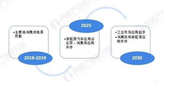 2018-2030 Evolution of Global GaN Power Electronic Devices Applications   ;
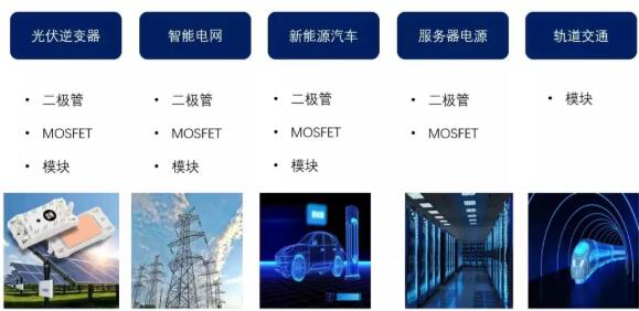
Technical difficulties and characteristics of GaN and SiC materials
At present, the third-generation semiconductor materials GaN and SiC have been recognized and highly concerned by the market. In the field of power semiconductors, industry insiders believe that, in addition to LED light-emitting and radio frequency, the technical difficulties of the third-generation semiconductor material SiC mainly lie in the control of substrate defects. At present, the substrate materials with low defect density are mainly produced by European, American and Japanese manufacturers, and it will take a long period of time to break through in China.
At the same time, the third-generation semiconductor material SiC process is difficult to control, and the product batch fluctuations lead to low yield and monopoly of main material supply. It is even deduced that the market price has remained high, and it is currently only limited to some application markets. However, compared with a series of its own characteristics such as lower loss, higher efficiency, high voltage and high temperature resistance of SiC, the application of the third-generation semiconductor material SiC has begun to change more industries.
Unlike SiC, GaN is relatively complex. GaN is not a MOSFET in the true sense, but a HEMT (High Electron Mobility Transistor), which has a switching characteristic similar to that of a MOSFET. GaN HEMT is a planar conductive structure that does not depend on the substrate and can be implemented on either sapphire or silicon substrates, but it is difficult to implement normally-off devices. Zhang Dajiang, Marketing Director of Zhuhai Gallium Future Technology Co., Ltd. ("Gallium Future" for short), believes that there are two solutions: one is to add P-type doping to the gate to block the two-dimensional electron gas and realize the normally closed function; One is to connect a low-voltage MOSFET in series with the source, and control the low-voltage MOSFET to provide the negative voltage turn-off of the GaN gate. The advantage is that the MOSFET has strong anti-interference ability.
In addition, the current technical difficulties of the third-generation semiconductor material GaN also come from many other aspects. In terms of process difficulty, GaN materials face challenges such as device yield, consistency, and reliability; for GaN companies, how can they improve the test content and process and screen out jobs for customers in the fastest and most accurate way? Good device; GaN's high heat resistance, high frequency resistance, low Vth and other characteristics are destined to have a different packaging direction from traditional silicon devices; at the same time, in application, the addition of the third-generation semiconductor material GaN has subverted the traditional power supply industry. The new power industry has higher requirements for PWM control chips and transformer manufacturers.
The reporter learned that Chengdu Nitrogen Silicon Technology Co., Ltd. (referred to as "Nitrogen Silicon Technology") has built a complete set of test lines after a long period of research and practice, which can not only select the normal working devices for customers, but also can test the devices. Classify, provide customers with cost-effective products that can meet the requirements, and use a large number of practical test data to help the foundry's process development to provide improvement directions. On the other hand, Nitrogen Silicon Technology vigorously researches advanced packaging and sealing technology to enhance the performance and ease of use of GaN devices; at the same time, it has contacted major manufacturers of transformers and PWM chips to develop solutions.
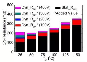
Yuan Weiwang, CEO of Xinmin Microelectronics (Shanghai) Co., Ltd. (referred to as "Xinmin"), believes that GaN is similar to silicon devices, and the internal resistance at high temperature shows an increase of more than 2 times the coefficient. Unlike silicon devices, switch During the process, the additional electrical stress causes the on-resistance to increase dynamically. Therefore, the technical difficulty of GaN devices mainly lies in how to deal with the different internal resistances caused by different usage time and ambient temperature, which are shown as follows:
1: RDson shows an unstable state as the temperature rises, as shown in the following figure:
Two: RDson also shows an unstable state over time, as shown in the following figure:
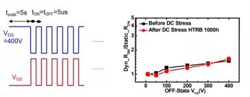
Based on the above-mentioned problems of GaN devices, the solution is to comprehensively consider the factors of thermoelectric stress, and consider using 3-3.5 times the RDson margin design. SiC devices are basically mature in the application of current Schottky diodes. The main problem is the stability of SiC MOSFETs, which requires long-term process debugging and exploration, and the technical difficulties have been basically overcome.
In addition to PD fast charging, GaN is attacking high-power power sources
Gallium Future is a leading GaN power device manufacturer in China, dedicated to the R&D and production of Cascode structure GaN products. According to reports, the structure combines the ease of use of silicon devices and the high-frequency and high-efficiency characteristics of GaN devices to achieve high power density power solutions up to 10KW. The products are mainly used for high-power server power supplies, base station power supplies, etc. Recently, Gallium Future has launched two small-size SMD cascode GaN devices for fast charging applications, G1N65R240PB and G1N65R480PA, corresponding to 65W and 33W fast charging applications respectively. With its strong anti-interference ability and simple driving method, it helps users to achieve Simple and efficient GaN fast charging design.
At present, the application of Nitrogen Silicon Technology's GaN power devices in consumer fields such as PD and LED power supplies has gradually matured. Manufacturers in white goods, as well as data centers, photovoltaics and other industries, and even in the field of automotive electronics have successively shown strong interest in GaN power devices from Nitrosil Technology. It is reported that in the future, Nitrogen Silicon Technology products will cooperate with self-developed GaN driver chips to gradually deploy a higher power and more stable GaN power device and module market.
The reporter learned that Xinmin GaN power MOS is mainly used in super fast charging, LED power supply and miniaturized high-density power supply. Among them, super fast charging is the main market of traditional GaN, while LED power supply, miniaturized high-density power supply, such as circuit breakers, micro base station power supply is an innovative field, and it is also the main layout market of Xinmin.
As the main market for the third-generation semiconductor material GaN, PD fast charging has gradually matured. In the future, high-power power supplies such as LEDs, base stations, and servers may become popular application markets for GaN materials.
SiC will shine in the automotive power supply market
Shenzhen Mipson Semiconductor Co., Ltd. ("Mipson" for short) has been committed to the development, production and promotion of the third-generation semiconductor material SiC since its establishment. The dual combination provides customers with more stable choices. At present, the company's SiC products have been maturely applied in the fields of PD fast charging, lighting power supply, photovoltaic inverter and server power supply; according to the different markets corresponding to the voltage segment, combined with the latest process technology, the key parameters are differentiated to make the products more suitable for users. Design. At present, MPS has supplied SiC MOS ultra-low internal resistance products in batches, and has the ability to share the market with imported brands, and continues to invest in research and development to bring more cost-effective options to customers through continuous improvement.
According to reports, MPS has actively deployed the rail transit and vehicle power supply markets in the field of third-generation semiconductor materials, and has reached agreements with a number of leading domestic car manufacturers, and some products have already started on-board trials.
At present, Xinmin's SiC devices are mainly used in inverters, including micro-inverters and high-power inverters. At present, the main products launched by Xinmin are SiC Schottky diodes and Schottky modules. It is reported that the third-generation semiconductor material market of Xinmin will mainly be deployed in high-efficiency and high-power power supply occasions such as charging piles and server power supplies.
As of this year, Tyco Tianrun Semiconductor Technology (Beijing) Co., Ltd. ("Tyco Tianrun") has been deeply involved in the field of SiC chips for ten years, and its products have been widely used in industries (such as high-power LED power supplies, PC power supplies, Communication power supply, photovoltaic inverter and charging module of charging pile, etc.), vehicle power supply (such as OBC, DCDC, etc.), consumer (such as PD fast charging) market.
Qiu Qi, vice president of marketing of Tyco Tianrun, believes that the future power supply direction is miniaturization, light weight and high power density, and emerging fields such as electric vehicles must be one of the main application fields of silicon carbide devices. Because if the electric vehicle motor electronic control adopts the full silicon carbide solution, an average of six silicon carbide six-inch wafers will be consumed. Power is also in new energy vehicles.
New energy vehicles require a large number of automotive electronic and electrical components. These devices play a very important role in the overall value, size, volume, dynamic performance, overload capacity, durability and reliability of the complete machine. As the dominant power device, silicon-based IGBT is used in the motor controller of new energy vehicles, and the motor and its controller account for about 7%-10% of the cost of the whole vehicle, which is the second highest cost component after the battery. The key device that determines the energy efficiency of the whole vehicle. At the same time, in order to achieve higher power density and high reliability, fast charging power devices need to have stronger performance, and a new generation of automotive power devices based on the third-generation semiconductor material SiC will also shine.
The process of domestic substitution will continue, and the cost will gradually decrease
From the out-of-stock wave in 2018, large foreign manufacturers focused on supplying foreign customers in unison, to the impact of the epidemic in 2020, the production bases of foreign manufacturers in Southeast Asia have been severely affected by production reductions, and domestic brand manufacturers have repeatedly undertaken the heavy responsibility of delivery. In addition, vigorously developing third-generation semiconductors has been upgraded to a national strategy. Combined with the huge domestic demand market, there is unprecedented space for localization and substitution, and it has also given the entire domestic third-generation semiconductor industry chain an opportunity to iterate.
This year, thanks to the support of the state and the unremitting efforts of the domestic semiconductor industry, the third-generation domestic semiconductors are growing at an incredible speed. In terms of third-generation semiconductors, the gap between domestic and foreign semiconductors is not as obvious as that of first- and second-generation semiconductors. As far as SiC diodes are concerned, domestic products have been basically localized and have entered the industrial and automotive fields; in terms of SiC Mosfet, there are still some gaps at home and abroad; in terms of GaN, my country's GaN RF equipment market scale is continuing to grow. The main pillars and main growth drivers are wireless communication infrastructure, etc. In terms of silicon-based GaN, it is now mainly used in mobile phone PD fast charging products, because consumer products are very cost-sensitive, and the technical threshold of the product itself is lower than that of industrial Class and vehicle class, the gap between domestic and foreign will no longer be obvious in the near future.
Yuan Weiwang predicts that in the next few years, SiC Schottky will be fully localized. At present, SiC MOS is still mainly based on ROHM in Japan, cree in the United States and STMicroelectronics and Infineon in Europe. The localization of MOS still requires further polishing of technical processes, but the long-term trend is still localization.
At present, the development direction of the third-generation semiconductor devices is clear, and domestic original factories occupy the right time and place. For the domestic third-generation semiconductor material SiC environment, in the past two years, under the pressure of the Sino-US trade war, foreign epidemics, and the shutdown of packaging factories in Southeast Asia, foreign manufacturers who took a wait-and-see attitude towards domestic manufacturers in the early years gradually opened their arms. Customers also have an open attitude to communicate with domestic original manufacturers. On the other hand, there is a deep bond between some foreign friends and European and American car manufacturers, and the supply capacity to other customers has declined. Due to insufficient supply, domestic benchmark customers will consider domestic semiconductors including domestic SiC.
Qiu Qi believes that, from 4 inches to 6 inches of silicon carbide materials and even 8 inches in the future, the cost of the third-generation semiconductor material SiC will drop, which will sink the segmented silicon market.
Yang Yong, product manager of Mipson, said that in the future, the gap between the third-generation semiconductor materials and the products of foreign manufacturers will become smaller and smaller, until they catch up or even surpass, and the price will definitely get closer and closer to the atmosphere. Ke Wei, the market manager of Nitrogen Silicon Technology, believes that within 3-5 years, the cost of domestic GaN power devices will inevitably approach the price of traditional silicon-based MOS and become the new darling of the market.
The process of domestic substitution of third-generation semiconductor materials still has a long way to go. Yuan Weiwang believes that in the current third-generation semiconductors, GaN devices are still dominated by Navitas, PI and gansystem in Canada. The industrial and automotive sectors still have a long way to go.
New direction for the development of third-generation semiconductor materials
As we all know, the purpose of using third-generation semiconductor materials is to improve product efficiency and power density. High-power products are mainly developed from Si IGBTs to SiC MOSFETs. At present, they have begun to be fully replaced in vehicle applications. The improvement of efficiency and the reduction of weight directly improve the battery life of electric vehicles. The small and medium power products are the development of Si MOSFETs to GaN HEMTs, and the main applications are data center power supplies and charging adapters.
The energy consumed by the data center accounts for about 10% of the total power generation. The power supply designed with the third-generation semiconductor material GaN can increase the efficiency by 3 to 5 points, thereby saving 3 to 5 thousandths of the country's electricity consumption. . This has very important implications for carbon neutrality. In terms of charging adapters, the use of gallium nitride can reduce the volume by half, and it has basically become a rigid demand for consumers. Especially with the introduction of PD3.1, in the future, you only need to bring a PD adapter to charge any portable electrical appliances. It's going to be a billion-dollar market.
Yang Yong believes that with the national "carbon neutrality" strategic tone and continuous support for the third-generation semiconductors, China will definitely lead the global third-generation semiconductor material SiC consumer market in the future. At the same time, as the domestic third-generation semiconductor material SiC process begins to mature gradually, and has been in stable production, it is believed that the problem of third-generation semiconductor materials can be fundamentally solved in the near future.
The trend of localization is unstoppable. The third-generation semiconductor is the main product of the country's overtaking in corners. With the advancement of technology, there will be a very broad market space. "The third-generation semiconductor materials are not only SiC and GaN, but also compounds such as gallium arsenide (GaAs) are also important forces in the future, and will have broad applications in the current 5G PA, power line broadband carrier and other fields." Yuan Weiwang said .
Conclusion
Driven by national policies and the support of the semiconductor industry, the third-generation semiconductor materials represented by GaN and SiC have become an important focus of the development of the semiconductor industry. Especially in the field of PD fast charging and new energy vehicles, the use of third-generation semiconductor materials GaN and SiC has greatly promoted product innovation and iteration. In view of the current status of domestic substitution, as domestic manufacturers continue to develop and innovate and break through technical difficulties, the position of the domestic third-generation semiconductor industry will occupy a place; The cost of semiconductor materials will also decline, and third-generation semiconductor materials such as GaN and SiC will be seen in many fields such as smart grids and rail transit for higher-power power supplies.
Disclaimer: This article is reproduced from "Electronic Intelligent Manufacturing Industry ", this article only represents the author's personal views, not Sacco Micro and the industry's views, only for reprinting and sharing, to support the protection of intellectual property rights, please indicate the original source and author. , if there is any infringement, please contact us to delete it.


Site Map | 萨科微 | 金航标 | Slkor | Kinghelm
RU | FR | DE | IT | ES | PT | JA | KO | AR | TR | TH | MS | VI | MG | FA | ZH-TW | HR | BG | SD| GD | SN | SM | PS | LB | KY | KU | HAW | CO | AM | UZ | TG | SU | ST | ML | KK | NY | ZU | YO | TE | TA | SO| PA| NE | MN | MI | LA | LO | KM | KN
| JW | IG | HMN | HA | EO | CEB | BS | BN | UR | HT | KA | EU | AZ | HY | YI |MK | IS | BE | CY | GA | SW | SV | AF | FA | TR | TH | MT | HU | GL | ET | NL | DA | CS | FI | EL | HI | NO | PL | RO | CA | TL | IW | LV | ID | LT | SR | SQ | SL | UK
Copyright ©2015-2025 Shenzhen Slkor Micro Semicon Co., Ltd
