Service hotline
+86 0755-83044319

release time:2022-03-17Author source:SlkorBrowse:13340
forward
There are many similarities between silicon carbide (SiC) device manufacturing technology and silicon manufacturing technology, but it is significant for this developing field to identify whether material differences will affect cleaning ability. Material differences include diffusion coefficient, surface energy and chemical bond strength, all of which can play a role in cleaning critical surfaces. In this work, the trace surface contamination level of 100 mm or 150 mm 4H silicon carbide wafer after mercury probe capacitance voltage (MCV) mapping was compared with that after subsequent cleaning. During MCV, trace metals such as mercury, iron and nickel were controllably added, and it was shown that various cleaning methods can restore the surface of silicon carbide to a cleanliness level lower than 5x10¹⁰ atoms /cm2. The position and cost comparison of these cleanings in the process flow of integrated devices are discussed.
Experiment and discussion
Mercury probe CV (MCV), TXRF and cleaning experiment
In order to controllably introduce pollutants into the surface of silicon carbide and test the cleaning ability, mercury detection was carried out on 100mm and 150mm epitaxial silicon carbide wafers with ultra-low microtubule density in Semerab MCV-530 tester, trace metal pollutants were measured by TXRF, the wafers were cleaned with various cleaning chemicals, and the trace impurities in the cleaned wafers were analyzed again. MCV measurement is carried out using multiple measurement modes, such as radius scanning, wafer mapping and multiple measurements at the same location, which enables the first TXRF measurement to compare the uncontaminated area with the contaminated area, and the post-cleaning TXRF to compare the pre-cleaning state.
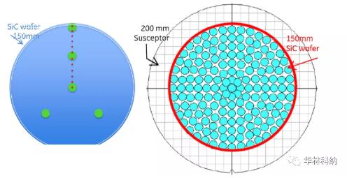
Figure 1. Layout of some models used in this study; In both cases, the position of TXRF of 50 mm silicon carbide wafer and about 10 mm diameter is displayed (the experimental mode of 100 mm silicon carbide wafer is not shown). Left: MCV 10-point radius scanning (~ 1.7mm diameter measuring point) allows 5-point TXRF measurement to analyze mercury-contaminated areas and mercury-free areas. Right: 165-point TXRF measurement on a 150mm 4H silicon carbide wafer displayed on a 200mm TXRF base.MCV, pre-cleaning TXRF and post-cleaning TXRF resultsAll cleaning has been proved to be effective in removing some degree of metal impurities. The mapped mercury level measured on a 100mm silicon carbide wafer with molybdenum anode TXRF showed that it decreased from the typical average value of 2.5x10¹³ atoms/cm2 and the typical maximum value of 2.4x10¹⁴ atoms/cm2 to the level below the detection limit of 300 seconds ~7x10¹⁰ atoms/cm2 immediately after the epitaxial test. RCA cleaning on 50 mm silicon carbide wafer has been proved to be effective in removing mercury, nickel, iron and other metals. The measurement results after cleaning are lower than the detection limit of concentrated RCA sequence, lower than that of diluted RCA sequence, but still measurable.Fig. 2 illustrates the comparison of mapped TXRF measured values before and after diluted RCA cleaning. Iron contamination on the surface was confined near the edge of the wafer before cleaning, and these locations could still be measured after cleaning with diluted RCA, although they were reduced. For the sake of yield and reliability, the cleaning trend can be observed on various interested metals (including mercury, iron and nickel), and the cleaning trend can be repeatedly observed on multiple wafers.
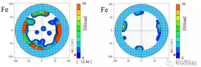
Figure 2. The iron contamination measured on the surface of 150mm 4H silicon carbide wafer was cleaned at 50℃ according to the RCA sequence of 1:2:50, each time for 5 minutes, in SC1&SC2 tank of DHF, and the cleaning time was 30 seconds. In the pre-cleaning stage, the iron concentration at the edge is high. Although the iron concentration in all areas decreases after cleaning, the concentration is still higher than the detection limit of this process.For the sake of yield and reliability, the cleaning trend can be observed on various related metals (including calcium, mercury, iron and nickel), and the cleaning trend can be repeatedly observed on multiple wafers, although some elements are completely cleaned to below the detection limit of TXRF using diluted dichloroacetic acid (titanium, chromium, copper and zinc). Fig. 3 illustrates the use of diluted RCA process to reduce the surface contamination of nickel. Again, it is noted that the concentration of nickel is higher at the edge of the wafer, and cleaning has made most areas lower than the detection limit of measurement.
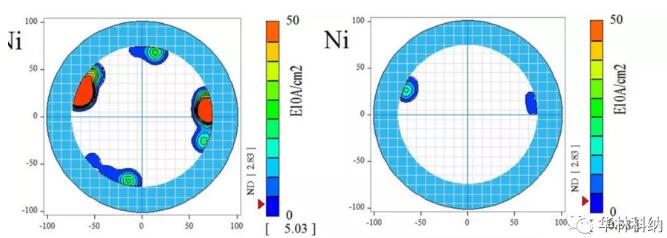
Figure 3. The surface-mapped nickel contamination measured before and after cleaning at 50℃ for 5 minutes (every SC1&2 tank, DHF step) on a 150mm 4H silicon carbide wafer in RCA sequence of 1:2:50 was performed for 30 seconds. In the pre-cleaning stage, the nickel concentration at the edge is high. Although the nickel in all areas decreases after cleaning, the nickel concentration is still higher than the detection limit in some places.
summary
Since it is known that RCA chemistry can remove pollutants by oxidizing silicon surface and removing oxides in hydrogen fluoride, this mechanism may not be realized on silicon carbide, because these chemicals are not expected to etch or oxidize silicon carbide at the temperature used in this work. In the previous work, it has been proposed that roughness plays a role in capturing metal pollutants, and hydrogen fluoride treatment results in the hydrophilic surface being mostly terminated by silicon hydroxide and carbon-oxygen groups. The results show that the diluted RCA with shorter time and lower temperature is not effective in removing iron, nickel and possible mercury. Although roughness may be a factor, the effect of temperature and time may indicate that the dissolution of metals (hydrochloric acid and NH4OH) in SC1 and SC2 chemistry is the main mechanism, but we suggest here that it can play a role through the diffusion of silicon hydroxyl and carbon-oxygen surface layer. It should also be noted that the exact mechanism of adding iron and nickel is still unclear, and the edge treatment of immersion box and/or the contamination of wafer manufacturing are the possible root causes. As the cost is greatly affected by time (affecting the output) and concentration (affecting the material cost and treatment cost), but less affected by temperature (only affecting the initial equipment cost), it is significant to explore the parameters for controlling the removal of metal pollutants in the future. It is also desirable to carry out this work in equipment capable of spray treatment, because a higher flow rate close to the wafer can achieve a high dissolution rate, which allows impurities to diffuse off the surface (15) more quickly. This effect has been well evaluated in polymer removal (16), and the evaluation of silicon carbide can also show its relationship with metal contaminants, although processing in this equipment may cause the surface contaminant value to be further lower than the TXRF detection limit.
Disclaimer: This article is reproduced from "Waring Kona". This article only represents the author's personal views, and does not represent the views of Sacco Micro and the industry. It is only for reprinting and sharing to support the protection of intellectual property rights. Please indicate the original source and author when reprinting. If there is any infringement, please contact us to delete it.
Company Tel: +86-0755-83044319
Fax/fax:+86-0755-83975897
Email: 1615456225@qq.com
QQ: 332496225 Manager Qiu
Address: Room 809, Block C, Zhantao Technology Building, No.1079 Minzhi Avenue, Longhua New District, Shenzhen


Site Map | 萨科微 | 金航标 | Slkor | Kinghelm
RU | FR | DE | IT | ES | PT | JA | KO | AR | TR | TH | MS | VI | MG | FA | ZH-TW | HR | BG | SD| GD | SN | SM | PS | LB | KY | KU | HAW | CO | AM | UZ | TG | SU | ST | ML | KK | NY | ZU | YO | TE | TA | SO| PA| NE | MN | MI | LA | LO | KM | KN
| JW | IG | HMN | HA | EO | CEB | BS | BN | UR | HT | KA | EU | AZ | HY | YI |MK | IS | BE | CY | GA | SW | SV | AF | FA | TR | TH | MT | HU | GL | ET | NL | DA | CS | FI | EL | HI | NO | PL | RO | CA | TL | IW | LV | ID | LT | SR | SQ | SL | UK
Copyright ©2015-2025 Shenzhen Slkor Micro Semicon Co., Ltd
