Service hotline
+86 0755-83044319

release time:2022-03-17Author source:SlkorBrowse:10548
If someone says to you, "Hey, the chip I made is 100% self-controllable!" Wait, don't be in a hurry to worship (believe) him first. Please read this article before you speak. ...

01
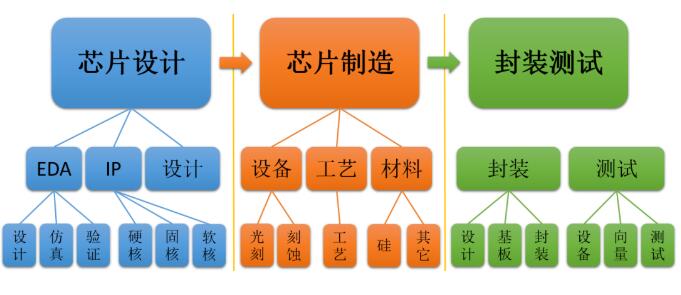
Chip design
1.1 EDA
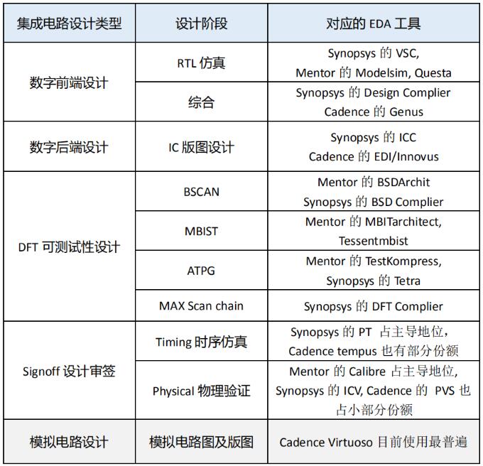
EDA(Electronic Design Automation) Electronic design automation, often refers to the software used for electronic design. Someone once said to me, "What's wrong with EDA? Isn't it just a tool?" Yes, it is a tool, but without it, you can't design anything! Today's large-scale integrated circuits can integrate more than 100 million transistors in a square millimeter the size of sesame seeds, and there are hundreds of millions of connecting networks among these transistors. Today's mainstream SoC chips have more than 10 billion transistors. If there is no accurate and powerful EDA tool, how can it be designed? EDA is an essential tool for chip design. At present, Synopsys, Cadence and Mentor(Siemens EDA) occupy more than 90% market share. In the design of high-end chips below 10 nanometers, its share is even as high as 100%. That is to say, it is almost impossible to develop a chip below 10nm without the EDA tools of the above three companies. The following table shows the current mainstream EDA tools in chip design:
1.2 IP
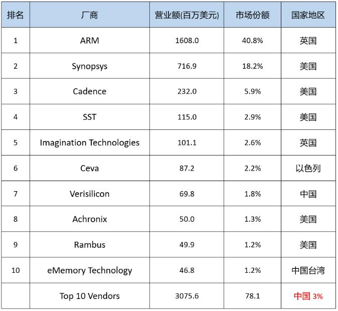
The following table shows the top 10 IP providers in the world at present. It can be seen that China has two finalists in the top 10, but the combined market share of the two companies is only 3%, while ARM alone accounts for more than 40% of the market share, while American enterprises account for 30% of the market share. If ARM is acquired by Nvidia, the IP market will basically be the world of the United States. In addition, we also find that Synopsys and Cadence, the two largest EDA companies in the world, also occupy the second and third positions in the IP field.
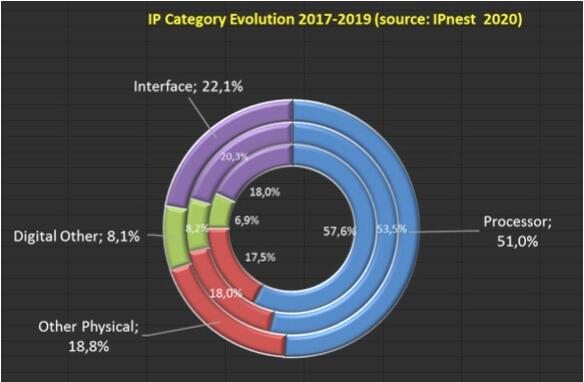
The following figure shows the types of IP, in which processor accounts for 51%, interface IP accounts for 22.1%, digital class accounts for 8.1% and others account for 18.8%. ARM, the processor class, is the only one. Synopsys is the industry leader in interface IP.
1.3design cycle
Chip design flow can be divided into digital IC design flow and analog IC design flow.Digital IC design process: chip definition → logic design → logic synthesis → physical design → physical verification → layout delivery.Chip Specification refers to making the function and performance index of the chip according to the requirements, and completing the design specification document.Logic Design refers to the realization of logic design at RTL(Register-Transfer Level) level based on hardware description language, and the correct function is verified by logic verification or formal verification.Logic Synthesis refers to the transformation of RTL into a gate-level netlist with a specific target, and the optimization of netlist delay, area and power consumption.Physical Design refers to the process of arranging and wiring the gate-level netlist according to constraints and finally generating the layout, which also includes: data import → layout planning → unit layout → clock tree synthesis → wiring.
Layout refers to the process of planning the positions of input/output units, macro units and other major modules on the chip.
Cell layout is the process of automatically placing standard cells according to netlist and timing constraints.
Clock tree synthesis refers to the process of inserting clock buffer, generating clock network and minimizing clock delay and deviation.Wiring refers to the process of automatically connecting each unit according to the circuit relationship under the constraint conditions of the number of wiring layers, line width and line spacing.
Physical Verificaiton usually includes layout design rule check (DRC), layout schematic diagram consistency check (LVS) and electrical rule check (ERC).
Tape Out refers to transferring layout files to the foundry to generate mask patterns and produce chips on the premise that all checks and verifications are correct.Analog IC design process: chip definition → circuit design → layout design → layout verification → layout delivery.
Among them, chip definition and layout delivery are the same as digital circuits, while analog IC is different in circuit design, layout design, layout verification and digital circuits.Analog circuit design refers to the design of transistor-level analog circuit structure according to system requirements, and the function and performance of the circuit are verified by SPICE and other simulation tools.
Analog layout design is to draw the layout geometry corresponding to the circuit diagram according to the design rules, and simulate the function and performance of the layout.
Analog layout verification is to verify the process rules, electrical rules and the consistency check of layout circuit diagram.Here, let's make a simple summary:
Chip design: With the support of EDA tools, the whole process of chip design is completed by purchasing IP authorization+independent research and development (cooperative development) IP and following the strict simulation and verification process of integrated circuit design. In this process, EDA, IP and strict design process are indispensable.
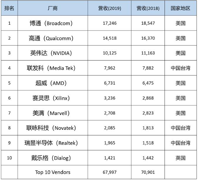
At present, among these three elements, the design process is the first one that can realize self-control.The following table lists the top 10 chip design companies in the world for your reference.
02
Chip manufacturing
2.1 equipment
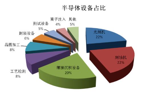
The manufacture of the chip needs more than 2,000 technological processes to complete, and each step depends on specific equipment to achieve it.There are three key processes in chip manufacturing: photolithography, etching and deposition. The three major processes are repeatedly circulated in the production process, and finally qualified chips are manufactured.Three key equipments are used in the three key processes, namely, mask aligner, etching machine and thin film deposition equipment. Three major equipments account for about 22%, 22% and 20% of all equipment investment, and they are the three semiconductor equipments with the highest proportion.
Take the most typical mask aligner and etching machine as examples to introduce and analyze the self-controllability.
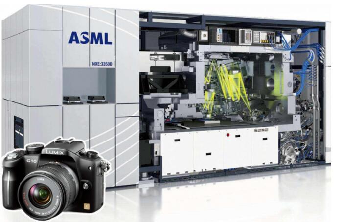
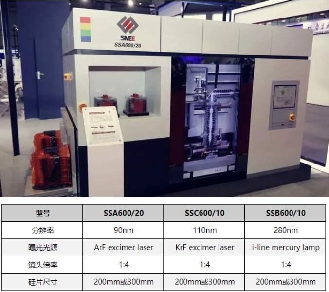
photoetching machine
Disclaimer: This article is reproduced from "The Analects of Confucius". This article only represents the author's personal views, and does not represent the views of Sacco Micro and the industry. It is only for reprinting and sharing to support the protection of intellectual property rights. Please indicate the original source and author when reprinting. If there is any infringement, please contact us to delete it.
Company Tel: +86-0755-83044319
Fax/fax:+86-0755-83975897
Email: 1615456225@qq.com
QQ: 3518641314 Manager Li
QQ: 332496225 Manager Qiu
Address: Room 809, Block C, Zhantao Technology Building, No.1079 Minzhi Avenue, Longhua New District, Shenzhen


Site Map | 萨科微 | 金航标 | Slkor | Kinghelm
RU | FR | DE | IT | ES | PT | JA | KO | AR | TR | TH | MS | VI | MG | FA | ZH-TW | HR | BG | SD| GD | SN | SM | PS | LB | KY | KU | HAW | CO | AM | UZ | TG | SU | ST | ML | KK | NY | ZU | YO | TE | TA | SO| PA| NE | MN | MI | LA | LO | KM | KN
| JW | IG | HMN | HA | EO | CEB | BS | BN | UR | HT | KA | EU | AZ | HY | YI |MK | IS | BE | CY | GA | SW | SV | AF | FA | TR | TH | MT | HU | GL | ET | NL | DA | CS | FI | EL | HI | NO | PL | RO | CA | TL | IW | LV | ID | LT | SR | SQ | SL | UK
Copyright ©2015-2025 Shenzhen Slkor Micro Semicon Co., Ltd
