In recent years, the research and application of ultra-wide bandgap semiconductor materials such as diamond, gallium oxide, aluminum nitride, boron nitride, etc. (bandgap > 4.5 eV) have continuously made technological breakthroughs. This kind of semiconductor material has higher bandgap, thermal conductivity and material stability. It has obvious advantages and great development potential in the fields of new generation deep ultraviolet electrical devices, high-voltage and high-power electronic devices, and is becoming a new hot spot in international competition.
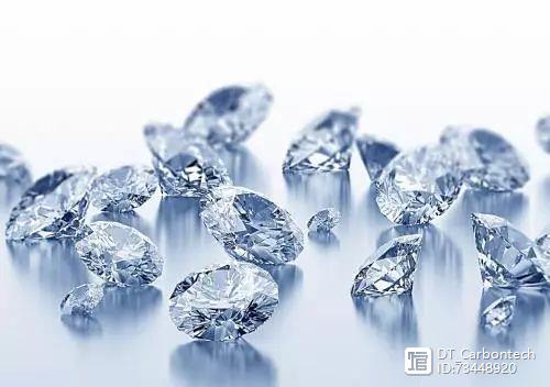 As a member of the ultra-wide bandgap semiconductor material (bandgap 5.5 e V), diamond has excellent physical and chemical properties, such as high carrier mobility, high thermal conductivity, high breakdown electric field, high carrier saturation rate and low dielectric constant. The following is a comparison of related parameters. Based on these excellent performance parameters, diamond is regarded as the most promising material for preparing the next generation of high-power, high-frequency, high-temperature and low-power-loss electronic devices, and is praised as the "ultimate semiconductor" by the industry. The regions that study diamond semiconductor materials and devices abroad are mainly Japan, the United States and Europe. The following is a detailed introduction. Comparison between diamond and other semiconductor properties

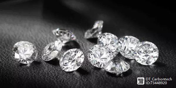
Development status of diamond semiconductor materialsPreparation of Diamond Diamond When diamond is used in semiconductor industry, it needs large-sized single crystal materials, and the preparation methods of diamond crystals are developing constantly, mainly by various CVD (chemical vapor deposition) technologies. In the 21st century, the appearance of repeated growth method, three-dimensional growth method and mosaic method has promoted the development of large-size diamond preparation, and once again set off the upsurge of research and preparation of diamond. The improvement of diamond material preparation technology is the driving force to improve the performance of diamond electronic devices. Internationally, British Elemental Six Company, Japan Industrial Technology Research Institute (AIST), Japan Material Research Institute (NIMS), Carnegie Institute of American Geophysical Laboratory, Argonne National Laboratory, etc. have been committed to the improvement of diamond material technology.

Elemental Six Company of UK is a leader in the synthesis of high-quality (electronic grade) CVD diamond single crystal, and it grew 5 mm× in 2004; 5 mm large-size electronic single crystal, the total impurity content can be controlled at 5ppb(ppb is one billionth), and the dislocation density is between 103 and 104 /cm2. It is the main supplier of high-quality single crystal for the development of diamond transistor, diamond quantum communication technology and diamond high-energy particle detector in the world. In many aspects, the commercial production of electronic grade 4-inch polycrystalline diamond has been realized.

In 2012, Carnegie Institute of the United States announced that it had made important progress in manufacturing carat colorless CVD diamond, and produced colorless single crystal diamond, which weighed 2.3 carats after processing and had a growth rate of 50μ m/h. Moreover, square diamond has been grown on six surfaces at the same time, which makes it possible to grow large single crystal diamond. In 2010, AIST Japan used MPCVD to prepare single crystal diamond with a size of 12 mm and mosaic wafer with a size of 25 mm. In 2013, AIST continued to expand the crystal size, and obtained 38.1 mm(1.5 inches) diamond pieces. In 2014, with the help of homoepitaxy technology and mosaic growth technology, 50.8 mm(2 inches) single crystal diamond was successfully obtained, but its impurity and dislocation density were high.

In 2017, the University of Augsburg, Germany, realized a large-size single crystal diamond material with a diameter of 92 mm and 155 carats by heteroepitaxy technology, which provided a new technical way for the development of large-size single crystal diamond. However, the dislocation density was high due to heteroepitaxy. The biggest problem of doping technology to realize the productization of diamond semiconductor devices is the difficulty of doping, especially N-type doping, and P-type doping is relatively easy. At present, boron-doped diamond P-type materials are basically mature and practical. However, this method requires high temperature (1450℃) heating, which will lead to the accumulation of multiple crystals, and the performance of the manufactured semiconductor devices is not as good as that of single crystals. If the doping of diamond single crystal is achieved by injecting boron atoms in the crystal production process, it will not only require higher injection power, but also reduce the performance of diamond crystal.
In 2016, the United States made a breakthrough in diamond doping technology, and developed a new low-temperature doping process, which can realize the doping of boron atoms in diamond single crystals at a lower temperature. It is simple, cheap and easy to operate. The core of the new process is the addition of "silicon", that is, a layer of boron-doped silicon is attached to a diamond single crystal, and then boron atoms can be transferred from silicon to diamond by heating to 800℃. By attaching silicon to a special position on the surface of diamond crystal, diamond with specific properties can be produced, thus realizing selective doping, achieving higher control force in device manufacturing, and pushing the development of diamond semiconductor devices one step further. Because this method realizes P-type doping, it still doesn't solve the problem of N-type doping. The next step will be to overcome the problem of N-type doping to realize transistors and other devices.
Research progress of diamond semiconductor devices
Diamond can be used as active device material to make FET, power switch and other devices, and can also be used as passive device material to make Schottky diode. Because of the high thermal conductivity and high charge mobility of diamond, the semiconductor devices made of diamond can be used in harsh environments such as high frequency, high power and high voltage, and have great application prospects. Some research progress has been made in the manufacture of diamond power electronic devices abroad, and some improvements have been achieved in key performance indicators. Since 2002, Japan has actively funded millions of dollars into the research field of diamond semiconductor devices, and has made some international leading progress.

In 2005, the diamond field effect transistor (FET) device developed by NTT Company of Japan has a linear gain of 10.94 d B, a power added efficiency of 31.8% and an output power density of 2.1 W/mm at 1GHz, which is the highest reported value at present. According to the new report, NTT has realized the development of 1 mm wide gate device at 1 GHz, with the output power of 1.26 W, gain of 17 d B and additional power efficiency of 56%. The next goal of NTT Company is to develop a diamond MESFET (Metal Semiconductor Field Effect Transistor) with a power density of more than 30 W/mm and a working frequency of 200 GHz, which can work in high temperature and harsh environment, and truly realize the replacement of high-power electronic vacuum tubes by solid-state electronic devices. In 2014, the research results published in IEEE in Japan stated that NO2 adsorption and Al2O3 passivation were used to solve the thermal stability of devices. The RF power FET made of hydrogen-terminated diamond with 100 nm gate length had current Ids=1.35 A/mm, ft=35 GHz, fmax=70 GHz, gate length and gate width of 0.2 μm and 390 μm respectively. The RF output power density is 2W/mm at 1 GHz, and it can work stably at 200℃. In 2017, Japanese researchers made a normally off C-H diamond MOSFET (metal oxide semiconductor field effect transistor) with a breakdown voltage of 2 k V by homoepitaxial growth of 500nm diamond film on (001) diamond substrate, and the gate threshold voltage Vth was 2.5 ~ 4 V. The preparation and application of electronic-grade diamond grown in American startup AKHAN Semiconductor Research Laboratory, according to reports, AKHAN has been authorized by the diamond semiconductor technology of Argonne National Laboratory of the U.S. Department of Energy. Combined with its own technological breakthrough in the diamond field, it is expected to become the first company in the world to truly realize the productization of diamond semiconductor devices. Akhan Semiconductor Company provided "Miraj Diamond Platform" as a solution to realize P-type and N-type devices, making it possible to manufacture diamond complementary metal oxide semiconductor (CMOS). The technical core of this process platform is that by doping P-type devices with phosphorus (P) and N-type devices with barium (Ba) and lithium (Li), two kinds of adjustable electronic devices with similar structure and performance are brought, and therefore diamond CMOS is developed. In addition, the strength and hardness of diamond glass produced by AKHAN for display and camera lenses are 6 times and 10 times that of Gorilla Glass, respectively. A The device manufactured by AKHAN's first diamond CMOS process is a diamond PIN diode with a thickness of only 500 nm, which is 10 times thinner than silicon, and its performance is 1 million times higher than that of silicon. Moreover, the PIN diode has no hot spot and parasitic loss, and its thermal performance is much better than that of silicon PIN diode. AKHAN Semiconductor Company owns several patents of diamond technology, covering the basic materials of almost all semiconductor components. Intellectual property rights can range from diodes, transistors and power inverters to full-featured diamond chips (such as integrated circuits). AKHAN Semiconductor Company also manufactured diamond electronic devices with a working frequency of 100 GHz and a characteristic size of 100 nm. Diamond has ultra-low resistance, reduces heat dissipation requirements, and can be deposited on silicon, glass, sapphire and metal substrates, which is expected to stimulate the evolution of microprocessor computing speed again. Research Other international research teams composed of French, British and Japanese researchers made new progress in diamond MOSFET in 2017, developed a new method of introducing deep depletion region into boron-doped diamond MOSFET, and constructed a new concept of diamond MOSFET.

When constructing MOSFET, researchers first deposited a layer of alumina (Al2O3) on the epitaxial layer of oxygen-terminated diamond at 380℃, and then doped the diamond layer with boron to form a stable depletion region. The epitaxial layer of diamond is functionally equivalent to a thick hole carrier channel. By applying a voltage to the gate, it can repel and deplete the hole carriers in the deep depletion region, thus controlling the on and off of the transistor. This new transistor operation mode makes the structure of diamond MOSFET simpler and reduces the manufacturing difficulty. The experimental results show that the new method can improve the carrier mobility of wide bandgap semiconductors by an order of magnitude. Subsequently, the researchers will conduct trial production of deep oxygen depletion terminated diamond MOSFET. In fact, more than a dozen teams in China have been engaged in the research of diamond semiconductor materials and devices, mainly the Institute of Semiconductors of Chinese Academy of Sciences, Institute of Metals of Chinese Academy of Sciences, Xi 'an Jiaotong University, xidian university, Jilin University, Zhengzhou University, Shandong University, Zhejiang University of Technology, Shanghai University, Wuhan Institute of Technology, etc., and have made progress in solar blind ultraviolet detectors.
Development prospect
With the continuous development of diamond semiconductor technology, the bottleneck problems such as N-type doping technology, large-size and high-quality single crystal preparation, high flatness and high uniformity material epitaxy technology will be broken through in the future, and diamond electronic devices with higher power performance will be realized. Diamond devices are thinner than silicon chips, and diamond-based electronic products are likely to become the industry standard of energy-efficient electronic products, which will have a significant impact on some high-tech industries, including faster supercomputers, advanced radar and telecommunications systems, ultra-efficient hybrid vehicles, electronic devices in extreme environments and the next generation of aerospace electronic devices. The content mainly comes from research and collation, and is for reference only.
With its excellent performance, diamond is widely used in high-end manufacturing industries such as precision tools, wear-resistant parts, coating of optical elements, processing of electronic products and accessories, etc. In addition, single crystal diamond is not only an "industrial tooth" but also an "ultimate semiconductor". The third generation wide bandgap semiconductors and devices represented by diamond are the foundation of the future development of integrated circuits in the information age, and have great application potential in many high-tech fields such as biological detection and medical treatment, flat panel display, environmental protection engineering and functional devices.
Based on this, the 4th International Carbon Materials Conference will focus on the research and exploration of high-end manufacturing and cutting-edge high-tech fields, besides focusing on the synthesis technology, doping technology and product production of diamond modules. Well-known experts, scholars and representatives of enterprises in the industry are invited to discuss new technologies, breakthroughs and developments, and open a new era for superhard materials to be applied in high-end fields.
Disclaimer: This article is reproduced from "DT_Carbontech". This article only represents the author's personal views, not those of Sacco Micro and the industry. It is only for reprinting and sharing to support the protection of intellectual property rights. Please indicate the original source and author when reprinting. If there is any infringement, please contact us to delete it.
Company Tel: +86-0755-83044319
Fax/fax:+86-0755-83975897
Email: 1615456225@qq.com
QQ: 3518641314 Manager Li
QQ: 332496225 Manager Qiu
Address: Room 809, Block C, Zhantao Technology Building, No.1079 Minzhi Avenue, Longhua New District, Shenzhen
 As a member of the ultra-wide bandgap semiconductor material (bandgap 5.5 e V), diamond has excellent physical and chemical properties, such as high carrier mobility, high thermal conductivity, high breakdown electric field, high carrier saturation rate and low dielectric constant. The following is a comparison of related parameters. Based on these excellent performance parameters, diamond is regarded as the most promising material for preparing the next generation of high-power, high-frequency, high-temperature and low-power-loss electronic devices, and is praised as the "ultimate semiconductor" by the industry. The regions that study diamond semiconductor materials and devices abroad are mainly Japan, the United States and Europe. The following is a detailed introduction. Comparison between diamond and other semiconductor properties


 In 2010, AIST Japan used MPCVD to prepare single crystal diamond with a size of 12 mm and mosaic wafer with a size of 25 mm. In 2013, AIST continued to expand the crystal size, and obtained 38.1 mm(1.5 inches) diamond pieces. In 2014, with the help of homoepitaxy technology and mosaic growth technology, 50.8 mm(2 inches) single crystal diamond was successfully obtained, but its impurity and dislocation density were high.


 Akhan Semiconductor Company provided "Miraj Diamond Platform" as a solution to realize P-type and N-type devices, making it possible to manufacture diamond complementary metal oxide semiconductor (CMOS). The technical core of this process platform is that by doping P-type devices with phosphorus (P) and N-type devices with barium (Ba) and lithium (Li), two kinds of adjustable electronic devices with similar structure and performance are brought, and therefore diamond CMOS is developed. In addition, the strength and hardness of diamond glass produced by AKHAN for display and camera lenses are 6 times and 10 times that of Gorilla Glass, respectively. A The device manufactured by AKHAN's first diamond CMOS process is a diamond PIN diode with a thickness of only 500 nm, which is 10 times thinner than silicon, and its performance is 1 million times higher than that of silicon. Moreover, the PIN diode has no hot spot and parasitic loss, and its thermal performance is much better than that of silicon PIN diode. AKHAN Semiconductor Company owns several patents of diamond technology, covering the basic materials of almost all semiconductor components. Intellectual property rights can range from diodes, transistors and power inverters to full-featured diamond chips (such as integrated circuits). AKHAN Semiconductor Company also manufactured diamond electronic devices with a working frequency of 100 GHz and a characteristic size of 100 nm. Diamond has ultra-low resistance, reduces heat dissipation requirements, and can be deposited on silicon, glass, sapphire and metal substrates, which is expected to stimulate the evolution of microprocessor computing speed again. Research Other international research teams composed of French, British and Japanese researchers made new progress in diamond MOSFET in 2017, developed a new method of introducing deep depletion region into boron-doped diamond MOSFET, and constructed a new concept of diamond MOSFET.
