Service hotline
+86 0755-83044319
release time:2022-03-17Author source:SlkorBrowse:13964
A diagram of circuit connection with circuit element symbols is called a circuit diagram. The circuit diagram is a kind of principle layout diagram drawn by people for the needs of research and engineering planning, which is based on physical and electrical standardized symbols. It can know the working principle of components, and provide a planning scheme for analyzing performance and installing electronic and electrical products.
Circuit diagram is one of the basic skills that electronic engineers must learn. This paper collects the classic circuit information related to regulated power supply, DCDC converter power supply, switching power supply, charging circuit and constant current source, and provides engineers with the freshest circuit diagram reference information, which is super complete and detailed, and can only help you here!
一、Regulated power supply
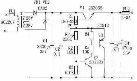
1、Circuit diagram of 3 ~ 25 V voltage adjustable voltage stabilization
The adjustable range of the regulated power supply is between 3.5V and 25V, and the output current is large. The regulated power supply adopts an adjustable regulator tube circuit, so as to obtain a satisfactory and stable output voltage.
Working principle: after rectification and filtering, the DC voltage is supplied to the base of the regulating tube by R1, which makes the regulating tube conductive. When V1 is conductive, the voltage goes through RP and R2 to make V2 conductive, and then V3 is also conductive. At this time, the emitter and collector voltages of V1, V2 and V3 do not change (their functions are exactly the same as those of the voltage stabilizing tube). By adjusting RP, a stable output voltage can be obtained, and the ratio of R1, RP, R2 and R3 determines the output voltage value of this circuit.
Component selection: transformer T is 80W~100W, with AC220V input and AC28V output. 1A for FU and 3a ~ 5a for FU2. 6A02 is selected for VD1 and VD2. RP 1W ordinary potentiometer with resistance value of 250K~330K, C1 3300µ F/35V electrolytic capacitor, 0.1µ for C2 and C3; F monolithic capacitor, C4 470µ F/35v electrolytic capacitor. R1 is 180 ~ 220Ω/0.1W ~ 1W, R2, R4 and R5 are 10KΩ and 1/8W. Choose 2N3055 for V1, 3DG180 or 2SC3953 for V2, and 3CG12 or 3CG80 for V3.
2、Circuit diagram of 3 ~ 15 V regulated and adjustable power supply
No matter how to repair computers or make electronic products, you can't do without a regulated power supply. Here's a regulated power supply with continuously adjustable DC voltage from 3V to 15V, and the maximum current can reach 10A. This circuit uses a high-precision standard voltage source integrated circuit TL431 with temperature compensation characteristics, which makes the regulated voltage precision higher. If there are no special requirements, it can basically meet the normal maintenance and use. See the following figure for the circuit.
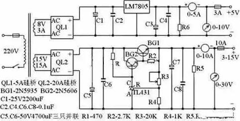
Its working principle is divided into two parts. The first part is a fixed 5V1.5A regulated power supply circuit, and the second part is another high-precision high-current regulated circuit with continuously adjustable routes from 3 to 15V.
The circuit of the first circuit is very simple. After the DC voltage rectified by the transformer secondary 8V AC voltage through the silicon bridge QL1 is filtered by C1 electrolytic capacitor, a fixed 5V1A regulated power supply can be generated at the output end by the 5V three-terminal voltage regulator LM7805 without any adjustment. This power supply can be used as an internal power supply when overhauling the computer board.
The second part is basically the same as the common series regulated power supply, except that the standard voltage source integrated circuit TL431 with temperature compensation characteristics and high precision is used, so the circuit is simplified, the cost is reduced, and the voltage stabilizing performance is very high.
In the figure, the resistor R4, the voltage regulator TL431 and the potentiometer R3 form a continuously adjustable constant voltage source, which provides the reference voltage for the BG2 base. The regulated value of the voltage regulator TL431 is continuously adjustable, which determines the maximum output voltage of the regulated power supply. If you want to expand the adjustable voltage range, you can change the resistance values of R4 and R3, and of course, the secondary voltage of the transformer should also be increased.
The power of the transformer can be flexibly controlled according to the output current, and the secondary voltage is about 15V. The rectifier QL for bridge rectifier is made of 15-20A silicon bridge, which has a compact structure and a fixing screw in the middle. It can be directly fixed on the aluminum plate of the casing, which is beneficial to heat dissipation.
What works is the high-current NPN silicon tube with metal shell. Because of its high calorific value, if the chassis allows, try to buy a large heat sink to expand the heat dissipation area. If you don't need a high current, you can also switch to a silicon tube with lower power, which can make the volume smaller.
Filter 50V4700uF electrolytic capacitors C5 and C7 are connected in parallel with three capacitors respectively, so that the output of large current is more stable. In addition, this capacitor should be bought with a relatively large volume, and those with a small volume should also be labeled as 50V4700uF as far as possible. When voltage fluctuates frequently or is not used for a long time, it is easy to fail.
Finally, let's talk about the power transformer. If you can't wind it yourself and can't buy a ready-made one, you can buy a ready-made switching power supply of more than 200W instead of the transformer. In this way, the voltage stabilizing performance can be further improved, but the manufacturing cost is not much different. Other electronic components have no special requirements, and they can work normally without much adjustment after installation.
二、Switching power supply
1、Working principle of integrated control IC-UC3842 for PWM switching power supply
The following figure shows the internal block diagram and pin diagram of UC3842. UC3842 adopts a fixed working frequency pulse width controllable modulation mode, and has 8 pins. The functions of each pin are as follows:
①It is the output end of the foot error amplifier, and the external resistor-capacitor element is used to improve the gain and frequency characteristics of the error amplifier.
(2) The pin is the input terminal of feedback voltage, which is compared with the reference voltage of 2.5V at the non-inverting terminal of the error amplifier to generate error voltage, thus controlling the pulse width;
③ Feet are the current detection input, and when the detected voltage exceeds 1V, the pulse width is reduced to make the power supply work intermittently;
④ The foot is the timing terminal, and the working frequency of the internal oscillator is determined by the external resistance-capacitance time constant, f=1.8/(RT× CT);
⑤ Feet are common ground;
⑥ The foot is push-pull output terminal, the inside is totem pole, the rising and falling time is only 50ns, and the driving capacity is ± 1A ;
⑦ The pin is the power supply end of DC power supply, which has the function of under-voltage and over-voltage locking, and the power consumption of the chip is 15mW;;
⑧ Feet are 5V reference voltage output terminal with 50mA load capacity.
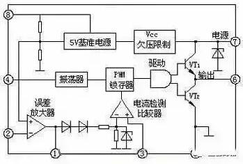
UC3842 internal principle block diagram
UC3842 is an integrated controller of PWM switching power supply with excellent performance, wide application and simple structure. Because it has only one output terminal, it is mainly used for switching power supply controlled by audio terminal.
UC3842 7-pin is the voltage input terminal, and its starting voltage range is 16-34V. When the power supply is started, VCC﹤16V, the input voltage of the comparator is 0, at this time, no reference voltage is generated, and the circuit does not work; When Vcc﹥16V, the input voltage Schmitt comparator sends a high level to the 5V fern voltage regulator, which generates a 5V reference voltage, which on the one hand supplies the internal circuit to work and on the other hand passes.
⑧ Feet provide external reference voltage. Once the Schmitt comparator is turned to high level (after the chip starts working), Vcc can be changed in the range of 10V-34V without affecting the working state of the circuit. When Vcc is lower than 10V, the Schmitt comparator turns to low level again, and the circuit stops working.
When the reference voltage source has 5V reference voltage output, the reference voltage detection logic comparator will reach a high level signal to the output circuit. Meanwhile, the oscillator will generate an oscillation signal of f=/Rt.Ct according to the external Rt and Ct parameters of the ④ pin, and this signal will be directly applied to the input of the totem pole circuit.
The other path is added to the setting terminal of the PWM pulse width RS trigger, and the R terminal of the RS PWN pulse width modulator is connected to the output terminal of the current detection comparator. Terminal R is the duty control terminal. When the voltage of R rises, the pulse width of terminal Q is widened, and the pulse width of terminal ⑥ is also widened (duty ratio increases); When the voltage at R terminal decreases, the pulse at Q terminal narrows, and the pulse width at ⑥ pin also narrows (duty cycle decreases).
The timing of each point in UC3842 is shown in the figure. Only when point E is at high level, and all points A and B are at high level, the high level will be sent to point D, and the low level will be sent to point C. Otherwise, the low level will be sent to point D and the high level will be sent to point C. ② Feet are generally connected to the output voltage sampling signal, also called feedback signal. ② When the foot voltage rises, ① the foot voltage will decrease, and the voltage at the R terminal will also decrease, so ⑥ the foot pulse will narrow; On the contrary, ⑥ the foot pulse becomes wider.
③ Feet are current sensing terminals. Usually, a small resistance sampling resistor is connected in series to the source or emitter of the power tube to convert the current flowing through the switch tube into voltage, and introduce this voltage into the feet. When the load short circuit or other reasons cause the current of the power tube to increase and the voltage on the sampling resistor exceeds 1V, ⑥ pin stops the pulse output, thus effectively protecting the power tube from damage.
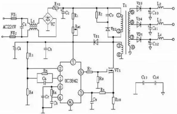
2、12V, 20W switching DC regulated power supply circuit composed of TOP224P
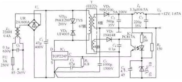
The 12V, 20W switching DC regulated power supply circuit composed of TOP224P is shown in the figure.
Two integrated circuits are used in the circuit: TOP224P three-terminal monolithic switching power supply (IC1) and PC817A linear optocoupler (IC2). The AC power is rectified and filtered by UR and Cl to generate DC high voltage Ui, which supplies power to the primary winding of high frequency transformer T.
VDz1 and VD1 can clamp the peak voltage generated by leakage inductance to a safe value and attenuate the ringing voltage. P6KE200 transient voltage suppressor with reverse breakdown voltage of 200V is used in VDz1, and UF4005 ultrafast recovery diode with 1A/600v is used in VDl.
The secondary winding voltage is rectified and filtered by V Φ, C2, Ll and C3, and the 12V output voltage Uo is obtained. The Uo value is set by the sum of the stable voltage Uz2 of VDz2, the forward voltage drop UF of LED in the optocoupler, and the voltage drop on R1.
Other output voltage values can be obtained by changing the turns ratio of high-frequency transformer and the regulated value of VDz2. R2 and VDz2 V also provide a dummy load for 12V output to improve the load regulation rate at light load. The feedback winding voltage is rectified and filtered by VD3 and C4, and then supplied to the bias voltage required by TOP224P. R2 and VDz2 are used to adjust the current at the control terminal, and the output duty ratio is changed to achieve the purpose of voltage stabilization.
共模扼流圈L2能减小由一次绕组接D端的高压开关波形所产生的共模泄漏电流。C7为保护电容,用于滤掉由一次、二次绕组耦合电容引起的干扰。C6可减 小由一次绕组电流的基波与谐波所产生的差模泄漏电流。C5不仅能滤除加在控制端上的尖峰电流,而且决定自启动频率,它还与R1、R3一起对控制回路进行补偿。
The main technical indicators of this power supply are as follows:
Input power grid frequency: FLL = 47 ~ 440 Hz;
Output voltage (io = 1.67a): uo = 12v;
Maximum output current: IOM=1.67A;;
Continuous output power: Po=20W(TA=25℃, or 15w (ta = 50℃);
Voltage regulation rate: η = 78%;
Maximum output ripple voltage: ± 60mV;
Operating temperature range: TA = 0 ~ 50℃.
三、DC-DC power supply
1、Circuit diagram from 3V to +5V and +12V
Portable electronic products powered by batteries generally adopt low power supply voltage, which can reduce the number of batteries and achieve the purpose of reducing the size and weight of the products. Therefore, 3 ~ 5V is commonly used as the working voltage. To ensure the stability and accuracy of the circuit, a regulated power supply is required.
If the circuit uses 5V working voltage, but needs a higher working voltage, it often makes the designer embarrassed. This paper introduces a circuit composed of two boost modules, which can solve this problem, and only needs two batteries to supply power.
This circuit is characterized by few peripheral components, small size, light weight, stable output of +5V and +12V, and meets the requirements of portable electronic products. +5V power supply can output 60mA, and the maximum output current of +12V power supply is 5mA.
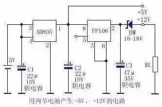
The circuit is shown in the above figure. It consists of AH805 boost module and FP106 boost module. AH805 is a boost module with 1.2 ~ 3V input and 5V output, which can output 100mA current when powered by 3V. FP106 is a SMD step-up module, with an input of 4 ~ 6 V and a fixed output voltage of 29± 1V, the output current can reach 40mA, and AH805 and FP106 are all level-controlled power-off control terminals.
The 3V voltage output by two 1.5V alkaline batteries is input to AH805, which outputs +5V voltage, one of which is 5V output, and the other is input to FP106 to generate 28 ~ 30v voltage, which is stabilized by a voltage stabilizer and outputs +12V voltage.
It can be seen from the figure that different output voltages can be obtained by changing the voltage stabilizing value of the voltage stabilizing tube, and the use is very flexible. Foot ⑤ of FP106 is the control power off terminal. When the power is turned off, the power consumption is almost zero. When the level of Foot ⑤ is raised to 2.5V, the power is turned on. When the low level of pin ⑤ is < 0.4V, the power supply is turned off. It can be controlled by circuit or manually. If no control is needed, the fifth foot is connected with the eighth foot.
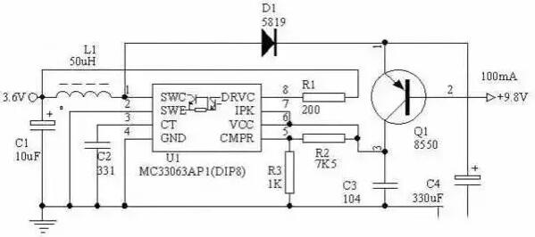
2、Make 3.6V to 9V circuit diagram with MC34063
functional mode:
No load: Input: 3.65V, 18uA (equivalent to 600mAH battery standby for more than three years)
Load: output: 9.88V, 50.2mA, input: 3.65V, 186.7mA, efficiency is 72%
Working principle:
This circuit can be used as a "4.2V to 5V mobile power supply without switching" with some improvements and increased power. You can use a battery box as a backup power supply for your mobile phone!
四、Charging circuit
1、Circuit diagram of lm358 alkaline battery charger
There are two different opinions about whether alkaline batteries can be charged. Some say it can be charged, and the effect is very good. Some say it can't be charged at all, and the battery description indicates that there is a danger of explosion. In fact, alkaline batteries can be charged, and the number of times of charging is generally about 30-50 times.
Actually, the mastery of charging method leads to two completely different consequences. First of all, there is no doubt that alkaline batteries can be charged. At the same time, in the description of batteries, it is mentioned that alkaline batteries cannot be charged, and charging may lead to explosion.
This is also true, but note that the word here is "may" cause an explosion. You can also understand it as a disclaimer of self-protection statement from the manufacturer. The key of alkaline battery charging is temperature. As long as the battery can be charged without high temperature, the charging process can be successfully completed. The correct charging method requires several points:
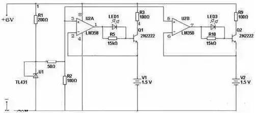
After some people try charging practice, they say categorically that they can't charge. The reasons why they can't charge electricity, use electricity for a short time, leak and explode are mostly the problems of chargers. If the charging current of chargers is too large, far exceeding 50ma, for example, the charging current of some fast chargers is above 200ma, the direct consequence is that the battery temperature is very high, which makes it hot to the touch, causing leakage in light cases and explosion in serious cases.Some people use Ni-MH rechargeable battery chargers to charge. Low-grade chargers don't have the function of automatically stopping charging. If the battery is overcharged for a long time, there will be liquid leakage and explosion. A better charger has the function of automatic charge stop, but the charge stop voltage is generally set to 1.42V of Ni-MH rechargeable battery, while the full charge voltage of alkaline battery is about 1.7V V.Therefore, if the voltage is too low, it feels like it can't be charged, and the electricity consumption time is short, which has no effect. Then there is the idea that the battery should not be discharged until the battery is completely dead before recharging. In this way, even the best battery can be recharged three or five times, and the effect is poor.Generally, it is recommended to use Nanfu alkaline battery with a voltage of not less than 1.3V Therefore, if you plan to charge alkaline batteries, you must have a qualified charger with a charging current of about 50ma and a charging cutoff voltage of about 1.7V V. Look at your charger.There are special chargers for alkaline batteries on the market, so-called patented products. Actually, it is a simple circuit with a charging voltage of 1.7V and a current of 50ma. Using the existing parts LM358 and TL431 at hand, I made a simple circuit. The cut-off voltage is 1.67V, which automatically stops charging. The cost is only two yuan. For the reference of interested friends.
Related description:
Alkaline manganese rechargeable battery: It is developed on the basis of alkaline zinc-manganese battery. It is also called mercury-free alkaline manganese battery because of the application of mercury-free zinc powder and new additives. This kind of battery can be charged and used dozens to hundreds of times without changing the discharge characteristics of the original alkaline battery, which is relatively economical.Alkaline-manganese battery is referred to as alkaline-manganese battery for short. It was successfully developed in 1882, developed in 1912, and put into production in 1949. It was found that when KOH electrolyte solution was used instead of NH4Cl as electrolyte, both electrolyte and structure changed greatly, and the specific energy and discharge current of the battery were significantly improved.
Its characteristics are:
The working temperature range is between-20℃ and 60℃, which is suitable for high and cold areas.
The capacity of heavy current continuous discharge is about 5 times that of acid Zn-Mn battery.
Its low-temperature discharge performance is also very good. The charging times are less than 30 times, generally 10-20 times, which requires a special charger, and it is extremely easy to lose the charging capacity.
2、Circuit diagram of 2.75W medium power USB charger
The LinkSwitch series product LNK613DG of Power Integrations is adopted in this design. This design is very suitable for mobile phone or similar USB charger applications, including mobile phone battery charger, USB charger or any application with constant voltage/constant current characteristics.
In the circuit, diodes D1 to D4 rectify AC input, and capacitors C1 and C2 filter DC. L1, C1 and C2 form a π-type filter to attenuate the EMI noise caused by differential mode conduction. These are related to the transformer E-sheild of Power Integrations? Technology, this design can easily meet the requirements of EN55022 B class conducted EMI with sufficient margin, and no Y capacitor is needed. Fire-proof, fusible and wound resistor RF1 provides serious fault protection and can limit surge current generated during startup.
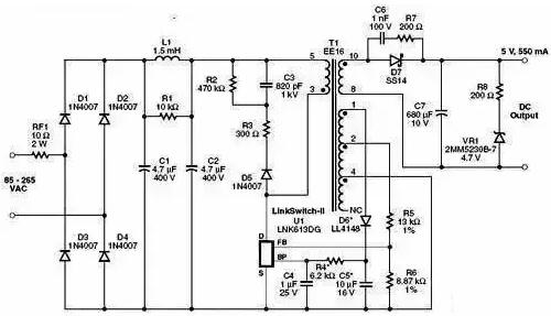
Figure 1 shows that U1 is powered by an optional bias power supply, which can reduce the no-load power consumption below 40 mW. The value of bypass capacitor C4 determines the amount of cable voltage drop compensation. The value of 1μF corresponds to the compensation of a 0.3 ω, 24 AWG USB output cable. (10 μF capacitor compensates 0.49ω, 26 AWG USB output cable. )
In the constant voltage stage, the output voltage is regulated by switch control. The output voltage is maintained by skipping the switching period. By adjusting the ratio of the enable period to the disable period, the voltage can be maintained. This can also optimize the efficiency of the converter in the whole load range. Under light load (trickle charging), the current limiting point will be lowered to reduce the magnetic flux density of the transformer, thus reducing the audio noise and switching loss. With the increase of load current, the current limiting point will also increase, and the skipped period will be less and less.
When no switching cycle is skipped (the maximum power point is reached), the controller in LinkSwitch-II will switch to the constant current mode. When the load current needs to be further increased, the output voltage will decrease. The drop of the output voltage is reflected in the FB pin voltage. In response to the voltage drop of FB pin, the switching frequency will drop linearly, thus realizing constant current output.
D5, R2, R3 and C3 constitute the RCD-R clamp circuit, which is used to limit the drain voltage spike caused by leakage inductance. The resistor R3 has a relatively large value, which is used to avoid the waveform oscillation of the drain voltage caused by leakage inductance, which can prevent excessive oscillation during the turn-off period, thus reducing the conducted EMI.
Diode D7 rectifies the secondary and C7 filters it. C6 and R7 can jointly limit the transient voltage spike on D7 and reduce the conducted and radiated EMI. Resistor R8 and Zener diode VR1 form an output dummy load, which can ensure that the output voltage at no-load is within an acceptable limit and that the battery will not be completely discharged when the charger is disconnected from AC mains. The feedback resistors R5 and R6 set the maximum operating frequency and the output voltage at the constant voltage stage.
五、constant flow source
1、How to design the driving circuit of three-wire constant current source
The constant current source drive circuit is responsible for driving the temperature sensor Pt1000, and converting its sensed resistance signal which changes with the temperature into a measurable voltage signal. In this system, the required constant current source should have the characteristics of constant output current, good temperature stability, large output resistance, output current less than 0.5ma (Pt1000 has no upper limit of self-heating effect), grounding at one end of the load, changeable polarity of output current, etc.
Because the temperature has less influence on the parameters of integrated operational amplifier than on the parameters of transistor or FET, the constant current source composed of integrated operational amplifier has the advantages of better stability and higher constant current performance. Especially when one end of the load needs to be grounded, it is widely used. Therefore, the dual operational amplifier constant current source shown in Figure 2 is adopted. The amplifier UA1 forms an adder and UA2 forms a follower. Both UA1 and UA2 are bipolar operational amplifiers OP07 with low noise, low offset and high open-loop gain.
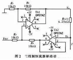
Let the potentials at the upper and lower ends of the reference resistor Rref in Figure 2 be Va and Vb, respectively, and Va is the output of the noninverting adder UA1. When resistors R1=R2 and R3=R4 are taken, Va=VREFx+Vb, so the output current of the constant current source is:
It can be seen that the dual operational amplifier constant current source has the following remarkable characteristics:
When the operational amplifier is powered by dual power supplies, the output current is bipolar;
The constant current can be realized by changing the input reference VREF or adjusting the reference resistance Rref0, so it is easy to obtain stable low current and compensation calibration.
Due to the mismatch of resistors, the voltage across the reference resistor Rref0 will be affected by the terminal voltage Vb of its driving load. At the same time, because it is a constant current source, Vb will definitely change with the change of load, which will affect the stability of constant current source. Obviously, this is unacceptable for high-precision constant current sources. Therefore, the selection principle of the four resistors R1, R2, R3 and R4 is that the mismatch should be as small as possible, and the mismatch direction of each pair of resistors should be consistent. In practice, a large number of precision resistors in the same batch can be screened, and four resistors with similar resistance values can be selected.
2、Circuit diagram of switching high withstand voltage constant current source
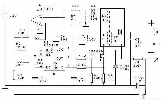
The development of the instrument requires a constant current source that can generate 1MA current on 0-3 mega-ohm resistor. A constant current source is designed with UC3845 combined with 12V battery. The transformer is a high-voltage package of color TV, in which L1 is wound around the core of the original high-voltage package for 24 turns, L3 with a coil of the original high-voltage package, and L2 with the high-voltage part of the high-voltage package. And L3 and LM393 constitute a voltage limiting circuit to limit the output voltage to be too high, and the open-circuit output voltage can be adjusted by adjusting R10.
Disclaimer: This article is reproduced from "Cloud Brain Think Tank". This article only represents the author's personal views, and does not represent the views of Sacco Micro and the industry. It is only for reprinting and sharing to support the protection of intellectual property rights. Please indicate the original source and author when reprinting. If there is any infringement, please contact us to delete it.
Company Tel: +86-0755-83044319
Fax/fax:+86-0755-83975897
Email: 1615456225@qq.com
QQ: 3518641314 Manager Li
QQ: 332496225 Manager Qiu
Address: Room 809, Block C, Zhantao Technology Building, No.1079 Minzhi Avenue, Longhua New District, Shenzhen



Site Map | 萨科微 | 金航标 | Slkor | Kinghelm
RU | FR | DE | IT | ES | PT | JA | KO | AR | TR | TH | MS | VI | MG | FA | ZH-TW | HR | BG | SD| GD | SN | SM | PS | LB | KY | KU | HAW | CO | AM | UZ | TG | SU | ST | ML | KK | NY | ZU | YO | TE | TA | SO| PA| NE | MN | MI | LA | LO | KM | KN
| JW | IG | HMN | HA | EO | CEB | BS | BN | UR | HT | KA | EU | AZ | HY | YI |MK | IS | BE | CY | GA | SW | SV | AF | FA | TR | TH | MT | HU | GL | ET | NL | DA | CS | FI | EL | HI | NO | PL | RO | CA | TL | IW | LV | ID | LT | SR | SQ | SL | UK
Copyright ©2015-2025 Shenzhen Slkor Micro Semicon Co., Ltd