Introduction to Semiconductor Packaging Technology
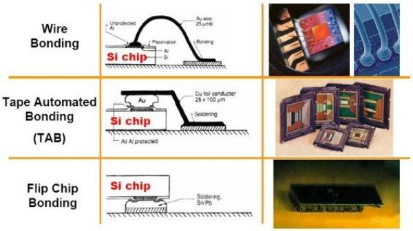
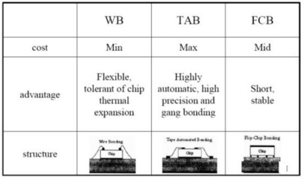
Those involved in the semiconductor industry, especially in semiconductor packaging, are inevitably familiar with several packaging processes, namely chip bonding, wire bonding, and flip chip bonding.
Among these, wire bonding and flip chip bonding are the most common. Tape Automated Bonding (TAB) technology is gradually being phased out in packaging due to its limitations.
Flip chip bonding technology involves interconnecting components by directly bonding the bumps on the chip downwards onto a substrate, carrier, or circuit board. In contrast, wire bonding connects the chip with the circuit board by placing the front side of the chip facing up and using wires (usually gold wires).
Wire bonding, Tape Automated Bonding, and flip chip bonding each have their own characteristics. Among them, flip chip bonding is becoming increasingly popular in the packaging industry due to its compact structure and high reliability.
What is Flip Chip Technology?
Flip chip technology originated from IBM, which developed the process of creating bumps on chips for flip chip soldering in 1960. The process involved surrounding the bumps with 95Pb5Sn encasing electroplated NiAu bumps. Later, PbSn bumps were used, employing Controlled Collapse Component Connection (C4) technology, initially developed for their large mainframe computers as a highly reliable packaging technique. C4 chips exhibit excellent electrical and thermal properties, with packaging fatigue life improved by at least ten times.
Following IBM's successful application of the C4 technology, subsequent technological advancements led some semiconductor companies to optimize and upgrade the C4 technology. This includes Fairchild developing Al bumps and Amelco introducing Au bump technology.
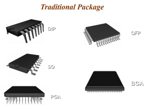
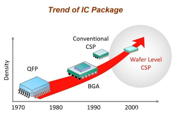
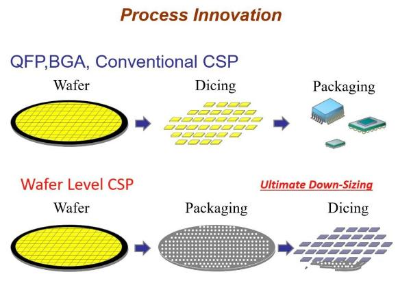
Semiconductor packaging technology has evolved from Quad Flat Package (QFP) to Ball Grid Array (BGA) packaging and to the latest Chip Scale Package (CSP) packaging.
The diagram below displays devices packaged using traditional QFP, BGA, and other technologies.
With the gradual reduction in the size of semiconductor chips, the demand for chip packaging technology is increasing, pushing packaging technology towards wafer-level and packaging development.
When packaging traditional chips, the usual process involves dicing the wafer into individual dies, followed by packaging each die separately. With the maturation of packaging technology, in the latest semiconductor packaging, there is a trend towards integrating packaging processes with semiconductor processes. This involves uniformly packaging chips on wafers before dicing them to create independent chips with higher reliability.
With the mature application of flip chip technology, the global consumption of flip chip components currently exceeds 600,000 units per year, growing at a rate of approximately 50%. 3% of wafer packaging is used for flip chip bumping technology, with expectations to exceed 20% in a few years.
Flip chip components are primarily used in semiconductor devices. Some components, such as passive filters, sensing antennas, and memory modules, are also beginning to adopt flip chip technology. As chips are directly connected to substrates and carriers through bumps, flip chip components are more precisely known as
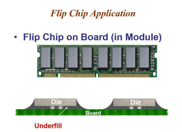
Direct Chip Attach (DCA). In the diagram below, electronic products like CPUs and memory modules are the most common devices that apply flip chip technology.
The diagram shows the connection between the memory chip and the circuit board in a memory module using flip chip technology, with the chip secured to the circuit board using underfill adhesive.
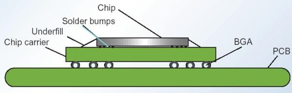
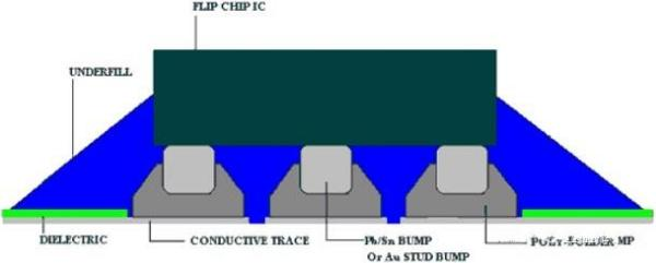
In typical flip chip packaging, the chip is connected to the chip carrier through 3 to 5 mils (1 mil = 25 micrometers) thick solder bumps, with underfill material at the bottom used to protect the solder bumps. The diagram below illustrates a typical flip chip interconnection, where the chip is connected to the substrate below using flip chip technology.
In the process of flip chip interconnection in semiconductor chips, there are many pre and post-processing steps. The following details elaborate on the flip chip technology process:
Step One: Under Bump Metallization (UBM)
The first step in flip chip interconnection is to create under bump metallization (UBM) on the chip surface. The essence of flip chip connection lies in the connection between the bumps on the chip and the bumps (pads) on the substrate. There are several ways to metallize the semiconductor surface:
(a) Sputtering: Thin films are deposited layer by layer on the silicon wafer using sputtering, followed by patterning the UBM layout through photolithography and etching away the non-patterned parts.
(b) Evaporation: Utilizing a mask, layers are deposited on the silicon wafer using evaporation. This selective deposition uses masks corresponding to the formation of the bumps.
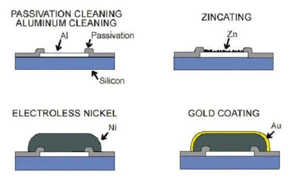
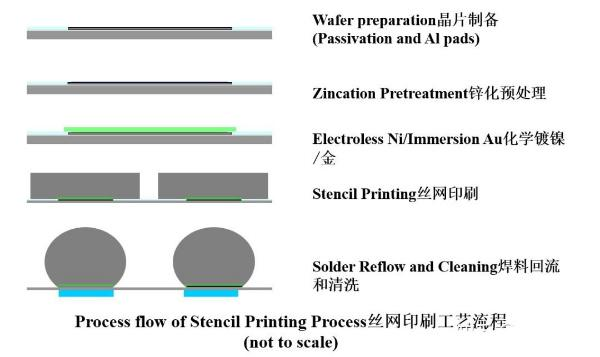
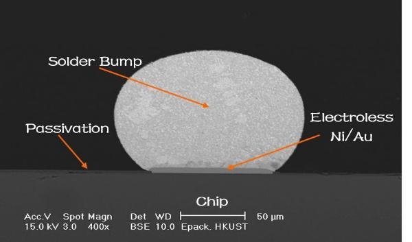
(c) Electroless plating: Nickel is selectively plated on Al solder pads using an electroless plating method. The Al surface is often treated with a zinc salt process. This method does not require vacuum or lithography equipment, resulting in lower costs. The diagram below illustrates the process of under bump metallization (UBM) on semiconductor chips.
Due to the presence of an oxide layer on the aluminum solder pad surface, metal plating cannot adhere to the oxidized surface. Therefore, it is necessary to appropriately treat the aluminum surface to remove the oxide layer.
A common method involves using zincation on the aluminum solder pad, where a layer of zinc is deposited on the aluminum surface to prevent oxidation. One drawback of the galvanizing process is that the aluminum can also be corroded by the plating solution. Hence, a secondary galvanizing process is required, during which about 0.3-0.4mm of aluminum will be corroded. In the galvanizing process, zinc deposits on the aluminum surface, while simultaneously the aluminum and aluminum oxide layer are corroded. The thin zinc layer protects the aluminum from further oxidation.
Following the galvanizing process, chemical nickel plating is further employed for UBM deposition, with metallic nickel serving as a barrier against diffusion/connection. Nickel has a very low diffusion rate and almost no reaction with the solder, making it ideal as the UBM metal for eutectic solder. Chemical nickel plating can be used for both UBM metal deposition and bump formation. Gold plating may be applied to some flip chip bumps, enhancing reliability due to gold's good conductivity and resistance to oxidation.
Step Two: Reflow to Form Bumps
There are various methods for forming solder bumps, including evaporation, electroplating, printing, stud bumping, ball drop, and solder transfer, with electroplating and printing being widely used.
After metallizing the bumps on the semiconductor surface, reflow ovens are used to form the flip chip bumps.
The general process of reflow to form bumps is illustrated in the diagram below.
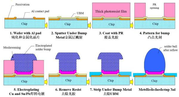
The specific process of forming solder bumps through electroplating is illustrated in the following diagram:
The commonly used material for bumps is the Pb/Sn alloy, as it exhibits good reflow soldering characteristics and is suitable for industrial production.
In addition to the commonly used Pb/Sn alloy, other bump materials such as Au/Ni alloy are also utilized. To ensure reliable interconnection, the Under Bump
Metallization (UBM) must be compatible with the alloy used for the bumps. A UBM suitable for high-lead content may not necessarily be suitable for high-tin solder. For instance, a Cu wetting layer is suitable for high-lead solder containing 3-5% tin, but it is not suitable for high-tin solder, as Cu reacts rapidly with Sn to form Sn-Cu intermetallic compounds. If the Cu is fully consumed, the solder will not wet the solder area.
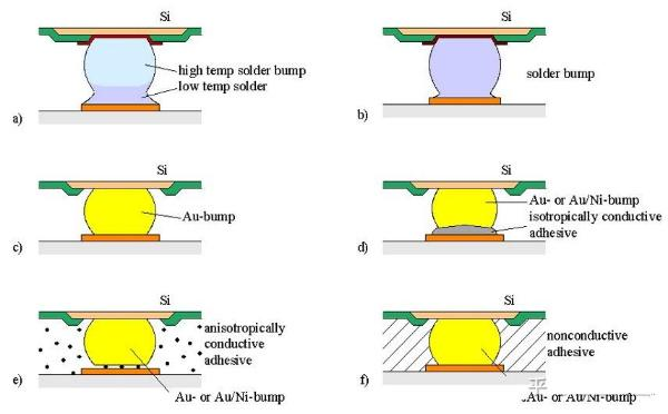
The diagram below illustrates flip chip connections with different bump materials.
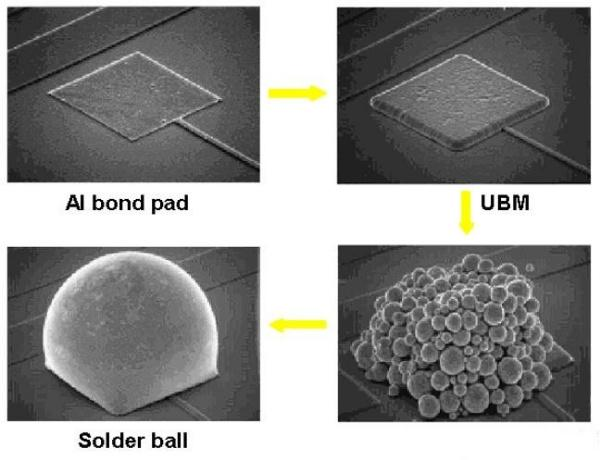
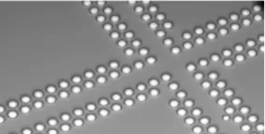
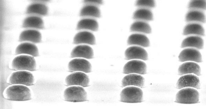
The appearance of the bumps formed on the surface of the chip as observed under a scanning electron microscope is shown in the diagram below:
The left image in the diagram shows the bump status before reflow (high temperature), while the right image depicts the bump status after exposure to high temperatures, where the bumps melt and form a spherical shape.
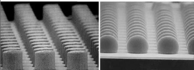
Chemical plating UBM and stencil printing processes are low-cost methods for bump preparation in industrial applications.
The following is the process flow for stencil printing of bumps and the appearance of bumps after completion.
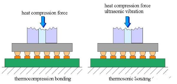
Step 3: Flip Chip Assembly
This process involves interconnecting the chips with completed bumps to the carrier substrate through flip chip bonding.
The most common method for connecting the chip to the carrier is the thermocompression bonding technique, with gold being the most suitable bump material.
Bumps can be generated using traditional electroplating methods or by employing stud bumping, a technique commonly used in wire bonding technology.
For thermocompression bonding, this process is only suitable for rigid substrates such as alumina or silicon, as it requires high pressure and temperature.
Additionally, the substrate must maintain high planarity, and the thermocompression head must exhibit high parallel alignment accuracy. To avoid unnecessary damage to semiconductor materials, a certain pressure gradient should be applied during the process.
Step 4: Underfill and Curing
After the flip chip bonding, the connection between the chip and substrate is established. To enhance the stability of the flip chip assembly, an underfill adhesive is applied between the chip and substrate. The underfill process is illustrated in the diagram below:
The bottom filling material between the chip and the substrate significantly improves the resistance to thermal fatigue, which would otherwise be the main reliability issue for flip-chip technology if there is no bottom filling.
(a) The bottom filling material disperses the concentrated stress to the chip's encapsulation material.
(b) It can prevent solder creep and increase the strength and rigidity of the flip-chip connection.
(c) It protects the chip from environmental influences such as moisture and ion contamination.
(d) It enables the chip to withstand mechanical vibration and shock.
In summary, the reliability of flip-chip connections is influenced by the coefficient of thermal expansion (CTE) mismatch between the substrate and the chip, as well as the height of the solder joints and the maximum spacing between them. Cracks in the connection area typically occur during the cooldown from the connection temperature.
Due to the high melting point of gold, it is less sensitive to fatigue damage compared to the solder. Therefore, as long as the stress during thermal cycling does not exceed the connection strength between the bump and the solder pad, reliability should not be a significant issue.
The bottom filling material between the chip and the substrate significantly improves the connection's resistance to thermal fatigue, and without it, thermal fatigue would be the main reliability issue for flip-chip technology.
Flip-chip assembly is particularly suitable for high-frequency applications because the connection path between the chip and the substrate is very short. The series impedance of flip-chip solder joints is about 1mW, and the series inductance is 0.025nH, much lower than the 5-10nH of wire bonding.
It is precisely due to these advantages of flip-chip assembly that the signal transmission delay can be significantly reduced.
Advantages and Disadvantages of Flip-Chip Technology:
Advantages:
(a) Small size: The small IC pin layout (only 5% of flat packages) reduces height and weight.
(b) Function enhancement: Using flip-chip technology can increase the number of I/Os. Unlike wire bonding, I/Os are not limited to the periphery of the chip. Area array can accommodate more interconnects in a smaller space for signals, power, and so on. Typical flip-chip pads can reach 400.
(c) Performance increase: Short interconnect distances reduce inductance, resistance, and capacitance, ensuring reduced signal delay, good high frequency performance, and better thermal paths from the chip's back.
(d) Improved reliability: Epoxy fill for large chips ensures high reliability. Flip-chips can reduce interconnect pin count by two-thirds.
(e) Enhanced heat dissipation: Flip-chips without encapsulation allow effective cooling of the chip's back.
(f) Low cost: Mass-produced bumps reduce costs.
Disadvantages:
(a) Bare chips are difficult to test.
(b) Limited adaptability of bumped chips.
(c) PCB technology faces challenges as spacing decreases and pin count increases.
(d) X-ray inspection equipment is necessary to detect invisible solder joints.
(e) Poor compatibility with SMT processes.
(f) Difficult handling of bare die.
(g) Requires high assembly precision.
(h) Current use of bottom filling requires a certain curing time.
(i) Some substrates have low reliability.
(j) Repair is difficult or impossible.
This concludes the introduction to flip-chip technology.